Chapter 8: The Only Arsenal — TSMC's Ultimate Monopoly
In the autumn of 2025, an NVIDIA supply chain manager sat in a cafe near the Hsinchu Science Park, waiting for his TSMC contact to reply to an email. The content of the email was simple: Could the production schedule for the next batch of B200 AI chips be moved up by two weeks?
He waited three days. The answer was no.
Not because TSMC didn't want to, but because ahead of NVIDIA on the production line were Apple's A19 Pro, AMD's next-generation EPYC server processors, Qualcomm's flagship mobile chips, and several clients whose names he was not permitted to know. Everyone was rushing them. Everyone felt their chips were the most important. But the factories in the world capable of manufacturing these chips—capable of etching tens of billions of transistors onto a twelve-inch wafer using a 3-nanometer process with a yield high enough for commercial mass production—there was only one.
Just this one.
Not in Silicon Valley. Not in Tokyo. Not in Seoul. Not in Berlin.
In Hsinchu.
The previous chapter described a four-layer-deep software prison—CUDA locking in hardware instruction sets, libraries, frameworks, and AI engineers worldwide. That prison is invisible; it is built out of code.
This chapter is about a tangible prison. Its walls are not code, but silicon, light, and hundreds of manufacturing processes precise down to the nanometer. The name of this prison is TSMC. And a significant portion of the bricks that built it—the process experiences that taught TSMC how to manufacture massive chips—were paid for by gamers.
I. An Uncomfortable Fact
Before unfolding the argument, let's get one thing straight.
The launch customer for TSMC's advanced processes is not gaming. It is Apple.
In September 2018, the Apple A12 Bionic became the first mass-produced TSMC 7nm chip. In 2020, the A14 Bionic pioneered 5nm. In 2022, the A16 Bionic debuted 4nm. In 2023, the A17 Pro debuted 3nm. With every generational shift in process technology, the iPhone is always the first to charge ahead.
In 2023, the revenue breakdown of TSMC's customers: Apple accounted for 25%, NVIDIA 11%, and AMD 7%. The biggest customer is Apple, not any company related to gaming.
This fact must be honestly acknowledged. The arguments in this book do not rely on hyperbole.
But numbers only tell half the story. Apple is TSMC's largest customer and most loyal launch partner—this is indisputable. However, the reason TSMC could become the only factory on Earth capable of mass-producing the most advanced chips does not rely on any single customer. It relies on an entire customer portfolio—and within this portfolio, the role played by gaming is far deeper than the revenue numbers suggest.
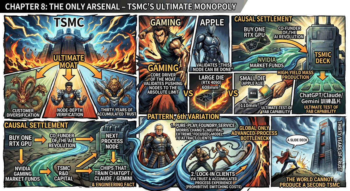
II. Four Types of Chips, Four Types of Exam Papers
To understand gaming's true contribution to TSMC, one must first understand something everyone in the semiconductor industry knows but rarely explains to outsiders: Not all chips are equally hard to make.
Every new process node at TSMC—for example, jumping from 7nm to 5nm—is like a newly built examination hall. The hall is built, but to verify if it works, you need examinees to come in and take a test. Different examinees take papers of different difficulty levels.
The Mobile SoC is the foundational paper.
Apple's A-series chips have a die area of about 110 square millimeters. Small chips, low power consumption, updated annually. Its requirement for TSMC is: prove that this new node can work—the transistors can function, the yield is high enough, and power consumption meets targets. This is the maiden voyage experiment. Apple is willing to pay top dollar to grab the first batch of capacity, and TSMC uses Apple's orders to recoup the cost of building the new node's fab. Both sides get what they need.
The Gaming GPU is the extreme paper.
NVIDIA's RTX 4090—the flagship consumer graphics card of 2022—houses a die of 608 square millimeters, 76 billion transistors, and consumes 450 watts. Using the exact same 5nm family process, Apple makes a chip the size of a fingertip, while NVIDIA makes a monster five and a half times larger than Apple's chip.
The difficulty of manufacturing a large die does not increase linearly—it increases exponentially. Defect distribution on a wafer is random; the larger the die area, the higher the probability of hitting a defect. A twelve-inch wafer yields fewer large dies, making the cost of each one higher. To get a 608-square-millimeter die to commercial mass production yields, TSMC's engineers must push the control precision of the entire process to its absolute limit—every photolithography exposure, every etching depth, the alignment of every layer of metal interconnects—all must be flawless.
Apple's A-series chips verified that "this node can make mobile SoCs." NVIDIA's and AMD's gaming GPUs verified that "this node can achieve the most extreme things." The former is an entrance exam; the latter is a stress test.
Without the stress test, TSMC wouldn't know how its process behaves under extreme conditions.
The Console SoC is the endurance paper.
The heart of the PlayStation 5 is a custom chip by AMD—a Zen 2 CPU plus an RDNA 2 GPU, produced on TSMC's 7nm. So is the Xbox Series X—the same architecture, the same foundry, the same process. Even the Steam Deck mentioned in Chapter 6 uses the AMD Aerith APU, also on TSMC's 7nm.
Three machines, one production line.
What makes consoles unique is their product cycle. The lifespan of a console generation is seven to ten years. Console manufacturers will not change chip suppliers during the entire lifecycle—you can't go to Sony three years after the PS5's launch and say, "Let's switch to Samsung." This means that what TSMC gets from Sony and Microsoft is an ultra-long-term, ultra-stable, predictable order.
The PS5 has shipped over 60 million units to date. The Xbox Series X/S over 30 million. The Steam Deck roughly 5.6 million. Inside every one of them is a TSMC 7nm chip.
The iPhone is an annual update—volume surges in September and begins to trail off the following March. This rhythm creates clear peaks and troughs in capacity utilization. What the console orders fill are exactly those capacity voids during the iPhone's off-season. They keep TSMC's fab utilization rate at a high level year-round—and a high utilization rate is the prerequisite for TSMC to continue pouring astronomical capital into building next-generation nodes.
The AI Training Chip is the harvest paper.
The NVIDIA H100, launched in 2022, drove the training of ChatGPT. TSMC N4 process—a refined version of 5nm. Die area over 800 square millimeters. Power consumption over 700 watts. A single card retails between $25,000 and $40,000.
How was the H100 built?
The N4 process it uses is the crystallization of TSMC's accumulated mass production experience in the 5nm generation. And the mass production yield of large 5nm dies—the number that determines whether "this 800-square-millimeter chip can be commercialized"—was verified by NVIDIA using the RTX 30 and RTX 40 series gaming graphics cards.
Gaming GPUs came first, the stress test was completed, and the large die process details were fine-tuned. AI chips came later, walking directly on the path paved by gaming GPUs.
Four exam papers, four contributions:
- Apple: Maiden experiment — "This node can work."
- Gaming GPUs: Stress test — "This node can be pushed to the limit."
- Console SoCs: Long-term orders — "This production line is worth keeping alive."
- AI Chips: Harvest — "The large die process verified by gaming is now used to make even larger dies."
Remove gaming, and this cycle loses two pieces—the stress test and the long-term orders. Without the stress test, TSMC wouldn't know how far its process could be pushed. Without long-term orders, TSMC's fab utilization wouldn't hold up, and investment decisions for the next node would waver.
AI chips did not fall from the sky. They grew standing on the shoulders of gaming GPUs.
III. The Moat of Trust
But a customer portfolio alone isn't enough. Is there a second foundry on Earth that can do advanced processes?
Yes. Samsung. And Intel is trying.
Samsung's advanced process technology, on paper, is not far behind TSMC's. Samsung's 3nm GAA (Gate-All-Around) transistors even reached mass production earlier than TSMC's. Under Pat Gelsinger, Intel introduced the Intel 18A process, publicly claiming its performance catches up to TSMC's N3.
But the reality in 2026 is: The world's most advanced AI chips, most advanced mobile processors, most advanced gaming GPUs—almost all are manufactured by TSMC. Samsung and Intel's combined market share in advanced processes is less than a fraction of TSMC's.
Why?
Not because Samsung and Intel's engineers are worse than TSMC's. It's because TSMC has a moat that other companies cannot replicate.
The name of this moat is trust.
Samsung's problem is called playing "both player and referee" in the industry. Samsung is the world's largest memory chip maker, the world's second-largest mobile phone brand, and simultaneously operates a foundry business. When a fabless chip company—like Qualcomm—hands over its most advanced chip blueprints to Samsung for manufacturing, a question arises in its mind: If Samsung's semiconductor division sees my design, will they leak critical information to Samsung's mobile phone division? Samsung's mobile phone division is competing directly with my clients.
Samsung pledges solemnly that there is a firewall between the two divisions. But solemn pledges do not make a moat.
Intel's problem runs deeper than Samsung's. Samsung's problem is "player and referee"—a conflict of interest. Intel's problem is its criminal record.
In 2003, AMD launched the Athlon 64 processor. From a purely technical standpoint, the Athlon 64 crushed Intel's contemporaneous Pentium 4—higher instructions per clock, lower power consumption, a more advanced 64-bit architecture. That was the only period in the history of x86 processors where AMD comprehensively led Intel in performance.
According to normal market logic, consumers should have voted with their feet, and AMD's market share should have skyrocketed.
It didn't.
Because Intel used a different set of logic.
Intel offered massive "exclusive rebates" to the world's largest PC brands—Dell, HP, Lenovo, Acer, NEC. The deal was simple: use only Intel CPUs, and I will give you hundreds of millions of dollars in subsidies; if you dare to stock a single AMD chip, the subsidies get slashed entirely.
Dell was the most extreme case. From 2003 to 2006, Intel paid Dell approximately $4.3 billion in exclusive subsidies. This money grew from 10% of Dell's operating profit in 2003 all the way to 38% in 2006. By the first quarter of 2007, it accounted for 76%. In other words—over three-quarters of Dell's profits came from Intel's subsidies, not from selling computers. Dell had transformed from a computer company into Intel's subsidy ATM.
In exchange, for those few years, Dell did not ship a single AMD desktop computer. Zero.
Not because AMD's products were bad—all benchmarks proved the Athlon 64 was faster. It was because Dell had done the math: using AMD chips might save a few dozen dollars in component costs per computer, but if Intel cut off over a billion dollars in annual subsidies, Dell's financials would instantly collapse.
In 2006, Dell finally began selling AMD computers. Intel retaliated immediately—slashing the subsidies. Dell's operating profit plummeted the next quarter.
In 2009, the European Commission hit Intel with a €1.06 billion antitrust fine—the largest fine against a single company in EU history at the time. That same year, Intel paid AMD $1.25 billion in a settlement. The US Federal Trade Commission (FTC) also filed a lawsuit in 2009, and in 2010 Intel signed a settlement agreeing to cease all exclusive rebate practices.
What does this history have to do with TSMC?
Everything.
In the early 2000s, Intel used channel bullying to maintain its monopoly in the x86 market. It didn't win on technology—its Pentium 4 lost to the Athlon 64 in performance. It won by using tens of billions of dollars in subsidies and threats to block AMD's sales channels.
This tactic worked in the short term. But it had a fatal side effect—it made Intel think it didn't need to go all-in on manufacturing.
Why bother catching up in process technology? The OEMs were all locked in by rebates anyway; even if AMD made a better chip, they couldn't sell it. Why consider spinning off the manufacturing business and embracing the fabless model? The "design plus manufacturing all-in-one" IDM model had always worked fine—relying not on manufacturing efficiency, but on channel control.
Intel's rebate case masked the fact that the IDM model was rotting from the inside. While Intel was busy using rebates to choke AMD from 2003 to 2007, TSMC was quietly doing something: upgrading from a "cheap foundry" to a "more advanced foundry than Intel." In 2018, when TSMC's 7nm entered mass production, Intel's 10nm was still struggling. That same year—Intel's process advantage, the core moat this company had maintained for over twenty years, officially flipped.
The sense of security bought by rebates ultimately caused Intel to miss the era shift in semiconductor manufacturing.
And this history had another consequence.
In 2009, the exact same year the Intel rebate case exploded, AMD made a desperate decision—to spin off its own foundries and establish GlobalFoundries. AMD didn't want to spin them off. It was forced to. Intel's rebate war pushed AMD to the brink of bankruptcy, and AMD could no longer afford to maintain its own fabs. Spinning them off was a matter of survival.
Ironically, this desperate decision for survival became the prerequisite for AMD's future rise.
After ditching its fabs, AMD became a pure design company—fabless. It could freely choose its foundries. In 2014, a newly appointed CEO named Lisa Su made a crucial decision: to hand over all of AMD's most advanced chips to TSMC. Zen architecture, RDNA architecture, PS5 SoCs, Xbox Series X SoCs, Steam Deck APUs—all manufactured by TSMC.
Intel used rebates to push AMD to bankruptcy → AMD was forced to ditch its fabs → AMD embraced TSMC → TSMC received AMD's orders, making its customer portfolio more diverse and its process experience denser → TSMC's virtuous cycle spun faster → Intel's own process was subsequently overtaken by TSMC.
Intel's rebate case was the biggest helper in TSMC's rise. It did two things: first, it paralyzed Intel in the comfort zone of IDM until it missed the process node transition; second, it forced AMD to become fabless, delivering to TSMC a super-customer that would later supply the hearts of all three major consoles.
This is the difference between "hegemony" (ruling by force) and "the king's way" (ruling by virtue). Intel relied on threats and rebates—"If you don't use my chips, I'll cut your subsidies." TSMC relied on trust and service—"Give me your core designs, and I will never compete with you."
Twenty years later, Intel wanted to pivot to the foundry business (IDM 2.0), knocking on the doors of NVIDIA, AMD, and Apple, asking if they were willing to let Intel manufacture their chips.
They looked at Intel's criminal record—a company that once bought off Dell with $4.3 billion in rebates and suppressed the entire OEM supply chain with threats—and politely said: No, thank you.
Intel said it would treat foundry customers fairly. But when a company with a history of bullying says "I'm a good guy now," compared to a company that has never had a conflict of interest since day one—who would you trust?
TSMC's genius lay in Morris Chang making what looked like the dumbest decision in 1987: not making its own products.
TSMC is a Pure Foundry. It does not design any chips, it does not sell any end products, and it does not compete with any customers. Apple hands the blueprints of the A-series to TSMC without worrying TSMC will use them to make its own phones. NVIDIA hands over GPU blueprints without worrying TSMC will make its own graphics cards. AMD, Qualcomm, Broadcom, MediaTek—every fabless chip company in the world can hand their core intellectual property to TSMC without any hesitation.
Because there is zero business overlap between TSMC and them. Zero.
This business model doesn't sound like some profound strategy. But its effect is: Every company in the world that wants to make the most advanced chips converges on the same foundry. Convergence brings diversity, diversity brings density of process experience, density of process experience brings yield advantages, and yield advantages bring more customers—a virtuous cycle spinning faster and faster.
What Samsung and Intel have to catch up to isn't just TSMC's technology. They have to catch up to the trust the global fabless ecosystem has accumulated in TSMC over thirty years. You can't catch up with a slide deck. You can't catch up in a quarter. You can't even catch up in a decade—because trust is not a technology that can be researched and developed; it is an irreversible ecological relationship.
IV. Gaming's Invisible Bill
Now we can string together the core argument of this chapter.
In early 2024, an AI research lab—maybe in San Francisco, maybe in London, maybe in Beijing—received a newly arrived batch of NVIDIA H100 GPUs. Engineers racked them up, connected them to the network, and began training a large language model.
They would never think about the following chain:
- The H100 is produced using TSMC's N4 process. N4 is a refined version of the 5nm family.
- The mass production yield of large 5nm dies was verified by NVIDIA using RTX 30 and RTX 40 series gaming graphics cards. The RTX 4090's 608-square-millimeter die and 76 billion transistors—among all chips of its generation, it was the most extreme stress test TSMC's 5nm process faced.
- Gamers paid $1,599 to buy an RTX 4090. A portion of that money became the foundry fee NVIDIA paid TSMC, became the engineering budget TSMC used to optimize large die yields, and became the process foundation that allowed the H100 to be mass-produced.
- During the same period, Sony and Microsoft placed long-term orders for tens of millions of console SoCs with TSMC annually. These orders filled the capacity utilization of TSMC's 7nm fabs, giving TSMC stable cash flow to invest in the next node. Every PS5 and Xbox Series X shipped was a stepping stone on TSMC's path to 3nm and 2nm.
- When TSMC's 3nm process matured enough to mass-produce AI chips, its large die process experience, its moat of customer diversity, and its fab utilization foundation—all had the fingerprints of gaming on them.
This is not a metaphor. It is the very real intersection of three threads: capital flow, engineering experience, and capacity planning.
The conclusion of Chapter 7 was: Every gamer who bought a GeForce is a co-funder of the AI revolution—their money nourished the software prison that is CUDA.
The conclusion of this chapter is the other half of that same sentence: Their money, simultaneously, nourished the physical arsenal that is TSMC.
Every cent NVIDIA collected in the gaming market became the R&D fund for TSMC to evolve the next-generation process. What gamers paid for wasn't just CUDA's software lock-in—they also paid for the silicon foundation that AI chips rely on to exist. Two independent mechanisms, the same group of victims, the same set of beneficiaries.
V. Closing Arguments
That pattern has appeared again. For the sixth time.
The prototype in Chapter 2: Microsoft uses DirectX's convenience to attract developers → Developers are locked into Windows → Consumers are locked in turn.
The variation in this chapter: Gaming verifies advanced processes → AI chips borrow gaming's process experience → Gamers become co-funders of the AI revolution.
But this time's variation has a crucial difference—the lock is not at the API layer, not at the software layer. The lock is at the physical layer.
DirectX's lock is built with code—so Valve could use another pile of code to bypass it. CUDA's lock is built by stacking four layers of software ecosystem—so AMD chased for ten years and still hasn't caught up.
TSMC's lock is structural.
What it locks is not an API, not a framework, not a knowledge system. What it locks is thirty years of trust from the global fabless ecosystem toward a single company, the process experience accumulated by dozens of clients on the same production line, and the irreversible ecological relationship created by a business model so simple it doesn't even sound like a moat: "We do not compete with our customers."
Samsung cannot catch up. Not because its engineers are bad—Samsung's semiconductor team is world-class. It's because its identity as both player and referee makes high-value clients like Apple, NVIDIA, and AMD too afraid to hand over their most advanced designs. Without these clients, Samsung's advanced processes lack the stress tests, the diversified experience, and the virtuous cycle.
Intel cannot catch up. Not because Pat Gelsinger's vision was wrong—the logic of IDM 2.0 works on paper. It's because Intel's conflict of interest in operating both CPU design and wafer foundry makes external clients distrust its priorities. The next chapter will tell Gelsinger's story—the tragedy of someone technically correct but disallowed by the system to execute.
The reason they can't catch up is not a technology gap. The reason they can't catch up is a trust gap. And a trust gap is something grown over time—you can't buy it with money, and spending time to chase it might not even work, because the person running ahead is still accumulating trust.
The lock in Chapter 6 is shallow—a single API layer, pryable. The lock in Chapter 7 is deep—four layers of software ecosystem, unpryable. The lock in this chapter is structural—it wasn't designed by any one person; it was grown unintentionally by an entire industry over thirty years. You wouldn't even know where to pry.
Three types of locks, three depths. So far, only the shallowest one has ever been pried open. And the one who pried it open—Valve—just built a new wall of its own.
This is the true face of technological hegemony. It is not a card game where you can turn the tables. It is a geological structure built layer upon layer—the topmost surface may occasionally be eroded by wind and rain, but the bedrock underneath remains completely unmoved.
VI. The Loot is Still Being Divided
Back to the NVIDIA supply chain manager at the beginning.
He waited three days, and TSMC's reply was: The production schedule cannot be moved up. Ahead in line are Apple, AMD, Qualcomm, and several clients he is not allowed to know the names of.
He treated this as a capacity management problem—"TSMC is too busy; they just need to expand their fabs next year."
No.
TSMC being "too busy" is not a capacity problem. It is a structural problem. Every company in the world that wants to make the most advanced chips is concentrated in the exact same factory—not because there are no choices, but because the only choice spent thirty years, brick by brick, building an fortress no one can replicate, using a business model that doesn't compete with you, using gaming GPUs for stress tests, using console SoCs for long-term orders, using Apple for maiden experiments.
And within this fortress, the easiest bricks to overlook—the 608-square-millimeter dies of the stress-test GPUs, the console chips filling the off-season capacity—all have the name of gaming carved into them.
The B200 order he placed with TSMC, every card his company sells to global AI labs, every cent of premium the global AI industry pays to wait in line for a silicon chip—all trace back to the same thread:
Someone wanted to play a better game.
That bill has not yet been settled. Moreover, the amount on the bill is inflating uncontrollably. Because for TSMC to continue building the next generation—2nm, 1.4nm—the required capital expenditure has surged to over $30 billion a year. A portion of this money will come from NVIDIA's revenue from selling gaming graphics cards. It will come from AMD's console contracts. It will come from the pocket of every gamer who spends $1,599 to buy an RTX 5090.
These gamers don't know what they are paying for.
They only know the new cards run faster, ray tracing looks more beautiful, and frame rates are higher. They discuss price-to-performance ratios in communities, discuss power consumption, discuss whether to wait for the next generation.
They don't know their money is nourishing an arsenal. And the things built inside that arsenal are reshaping the direction of human civilization.
But the bill is not just money. There is another side to the bill.
Every chip TSMC builds—whether it's for an iPhone, a PlayStation, a Steam Deck, or an H100—needs someone to design it. Designing GPU architectures is the job of NVIDIA and AMD. Designing console SoCs is the job of AMD. And the reason AMD can simultaneously design the chip for the PS5, the chip for the Xbox Series X, and the chip for the Steam Deck—the hearts of all three major platforms coming from the exact same company—is because someone made a decision a decade ago that everyone laughed at.
That person's name is Lisa Su. That decision was to abandon AMD's own fabs and fully embrace TSMC.
That is the story of the next chapter.